
Semiconductor Materials and Their Properties
Semiconductor Materials and Their Properties
Semiconductor materials lie between metals and dielectrics (insulators). They possess distinctive electrical and physical properties that endow semiconductor devices and circuits with unique behavior. A defining feature is tunability via doping—introducing specific impurities to modify and control electrical performance. The importance of semiconductor materials in chip manufacturing is self-evident. This article surveys their historical development, classifications, and key properties.
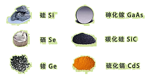
Development of Semiconductor Materials
First-Generation: Elemental Semiconductors
Since the 1950s, first-generation materials represented by silicon (Si) and germanium (Ge) supplanted bulky vacuum tubes, catalyzing the rise of microelectronics centered on integrated circuits and propelling the broader IT industry. Ubiquitous products such as CPUs and GPUs owe their existence to these materials. In short, first-generation semiconductors laid the foundation of modern microelectronics.
Second-Generation: III–V / II–VI Compound Semiconductors
Defined by direct bandgaps and high carrier mobility, these include GaAs, InP, AlGaAs, InGaAs, and related alloys. Their bandgaps are widely tunable via alloying (typical GaAs Eg=1.42 eV). In the 1960s, limitations of indirect-gap Si—low radiative recombination efficiency and, in some cases, less favorable breakdown and high-frequency performance—restricted its use in high-efficiency light emission and certain high-frequency/high-power scenarios. Compound semiconductors, exemplified by GaAs, opened the optoelectronics era, notably in infrared lasers and red LEDs based on AlGaInP/GaAsP grown on GaAs substrates. They also enabled millimeter-wave devices, satellite and mobile communications, GPS, etc. With the surge in demand for 4G communications equipment, second-generation materials underpinned a solid infrastructure for the information industry.
Third-Generation: Wide-Bandgap Semiconductors
Represented by SiC and GaN, these materials feature wide bandgaps (~3.0 eV). From the 1980s onward, the industry sought devices with high voltage tolerance, high-temperature capability, high power handling, radiation hardness, higher conductivity, faster operation, and lower losses. SiC and GaN deliver high breakdown fields, good thermal performance/high-temperature operation, and high critical current-carrying capability, making them ideal for high-voltage, high-power, and high-frequency applications such as automotive traction inverters, fast chargers, energy storage and PV inverters, and RF (radar/5G). They can significantly improve energy conversion efficiency and reduce system-level cost, with broad prospects in defense, aerospace, new-energy vehicles, and PV/storage.
Snapshot of the Three Generations
Generation | Representative Materials (Mainstream) | Core Characteristics | Typical Applications (Examples) |
First-Gen (Elemental) | Si, Ge | Mature processes, low cost; Si is an indirect bandgap material | Logic/memory/analog ICs; power devices (superjunction MOSFETs, IGBTs); silicon photodetectors; crystalline-Si PV |
Second-Gen (Compound) | III–V: GaAs, InP, AlGaAs, InGaAs; II–VI: CdTe, ZnSe | Direct bandgaps + high mobility; bandgap/lattice tunable via alloying | Light emission & lasers (IR/visible, 1.3/1.55 µm), high-speed optical-communication devices, IR detection; RF front-ends (pHEMT/HBT); high-efficiency GaAs space solar cells |
Third-Gen (Wide Bandgap) | SiC, GaN (mainstream); candidates: AlN, c-BN, diamond, ZnO | Wide bandgaps → high breakdown field, high thermal performance, high-temperature/ high-field capability | SiC: >600 V high-voltage/high-power (EV main inverters/chargers, PV/storage inverters, industrial PSUs). GaN: ≤650–900 V high-frequency fast switching (adapters/server PSUs) and RF PAs (5G, radar); GaN LEDs/LDs at scale |
- In semiconductor materials, “first/second/third generation” is an application-oriented engineering taxonomy, not an ordinal performance ranking. Si and compound semiconductors are complementary: Si dominates most ICs and many power devices thanks to its mature ecosystem and cost; III–V materials (e.g., GaAs, InP) dominate light emission, lasers, detection, and high-frequency RF due to direct bandgaps and high mobility. Industry practice often leverages heteroepitaxy/bonding or package-level system integration (e.g., Si CMOS + GaAs RF, Si control + SiC power, silicon photonics + InP lasers) to combine strengths.
- Third-generation (SiC/GaN) does not “fully replace” earlier generations. It is rapidly penetrating and partially displacing older solutions in >600 V high-voltage/high-power and ≤650–900 V high-frequency fast-switching & RF domains, boosting efficiency and power density. For logic/memory, cost-sensitive low-voltage power, and optical-comm lasers, Si or second-generation materials remain optimal. The future is division of labor + heterogeneous integration, not wholesale substitution.
Key Performance Parameters of Representative Semiconductors
Material | Bandgap Eg (eV) | Relative Permittivity εr | Critical Breakdown Field Ec (MV/cm) | Electron Saturation Velocity vsat (107cm/s) | Thermal Conductivity (W/cm·K) | Electron Mobility μn (cm²/V·s) |
Si | 1.12 | 11.7 | ~0.3 | ~1.0 | ~1.5 | ~1350 |
GaAs | 1.42 | ~13.1 | ~0.4 | ~2.0 | ~0.46 | ~8500 |
InP | 1.34 | ~12.5 | ~0.5–0.6 | ~2.0 | ~0.68 | ~5400 |
4H-SiC | 3.26 | ~9.7 | ~2.5–3.5 | ~2.0 | ~4.5 | ~900 |
GaN | ~3.4 | ~9.0–9.8 | ~3.0–3.5 | ~2.0–2.5 | ~2.0–2.5 | ~1000 |
Note: Values vary with polytype/epitaxy/defects and test conditions; the table provides commonly cited ranges.
Classifications of Semiconductor Materials
By application
- Microelectronics/Information ICs; Power electronics; Optoelectronics (incl. photovoltaics); Sensing & imaging (IR, X/γ-ray, etc.).
By crystalline order
- Single-crystal / polycrystalline / amorphous (microcrystalline and 2D layered materials are often listed separately).
By morphology
- Bulk wafers/ingots / epitaxial thin films / nanostructures (quantum wells/wires/dots, nanowires, powders).
By composition
- Inorganic semiconductors
Elemental: Si, Ge, C (diamond), Se, Te, black phosphorus (an allotrope of P), etc.
Compound:
III–V: GaAs, InP, GaN, AlN, AlGaAs, InGaAsP, …
II–VI: CdS, CdSe, CdTe, ZnO, ZnSe, HgCdTe, …
IV–IV: SiC, SiGe, …
IV–VI: PbS, PbSe, PbTe, …
Oxides/Halides: Ga₂O₃, In₂O₃, SnO₂, IGZO, TiO₂, Cu₂O (halide perovskites are organic–inorganic hybrids; see below).
- Organic semiconductors: small-molecule and polymer systems (OLED, OPV, OFET).
- Organic–inorganic hybrids: halide perovskites (e.g., CH₃NH₃PbI₃ etc.).
Typical Room-Temperature Resistivity ρ (Ω·cm)
Category | Typical Range of ρ | Examples (approx.) |
Insulators | ≳ 1010–1014 (ultra-pure up to 1016–1018) | Glass ~1011–1013; fused silica ~1016–1018; high-purity diamond ~1013–1016 |
Semiconductors | 10-2–108 (heavily doped to ~10-4 | Intrinsic Ge ~10-2–102; Si (doping-dependent) ~10-3–105; compounds such as GaAs and CdS also span multiple decades |
Metals | 10-6–10-4 | Ag 1.6×10⁻⁶; Cu 1.7×10⁻⁶; Al 2.7×10⁻⁶; Pb 2.2×10⁻⁵; Hg 9.6×10⁻⁵ |
At room temperature, typical semiconductor resistivity is about 10−2 to 108Ω⋅cm (down to ≈10−4 Ω⋅cm under heavy doping), intermediate between insulators and metals. Conductivity is governed jointly by carrier concentration and mobility: doping and illumination increase carrier density and thus lower ρ. Across common engineering temperatures, stronger lattice vibrations reduce mobility, so ρ rises slightly; as temperature increases further into the intrinsic regime, thermally generated carriers proliferate and ρ drops sharply. Under strong electric fields, velocity saturation and potential breakdown occur, so the I−V relation ceases to be linear. Defects and grain boundaries raise ρ by enhancing scattering and recombination.
Electrical Conductivity of Metals, Semiconductors, and PN Diodes (Room Temp ≈ 25 °C)
Metals conduct readily primarily because they contain a very high density of free electrons; as a result, voltage and current are approximately linear (Ohmic behavior). As temperature rises, lattice vibrations intensify, scattering increases, and the resistance rises slightly.
Semiconductors support conduction by both electrons and holes, giving a conductivity between metals and insulators yet amenable to control: doping (introducing acceptors/donors) or illumination (creating electron–hole pairs) can substantially increase the carrier population and thus enhance conduction. Within common engineering temperature ranges, increasing temperature mainly reduces mobility (more scattering), so resistance rises slightly; at higher temperatures, once the intrinsic regime dominates, thermally generated carriers proliferate and the resistance drops sharply. A PN diode, formed by joining p-type and n-type regions, is rectifying: under forward bias it turns on beyond a threshold (≈0.6–0.7 V for silicon devices); under reverse bias only a small leakage flows until excessive voltage causes breakdown and a sharp rise in current.
Overall, how well a material conducts depends on how many carriers there are (concentration) and how fast they move (mobility); temperature, illumination, strong electric fields, and defects/grain boundaries all modify these two factors and hence the observed conductivity.
Room-Temperature Conductivity Overview
Type | Primary Carriers | Conductivity (Room Temp) | External Influences (Temperature / Light / Field) | Features |
Metals (e.g., Cu, Al) | Mainly electrons | Very good (low resistance) | ↑T → resistance slightly ↑; light has negligible effect; field–current relation largely linear | Natural good conductors; used for wiring/enclosures |
Semiconductors (e.g., Si, GaAs) | Electrons and holes | Between metals and insulators; tunable | Doping/illumination → more conductive; in common ranges ↑T → resistance slightly ↑; at higher T (intrinsic) resistance ↓; strong fields may cause nonlinearity/breakdown | “Programmable conductors” for transistors, sensors, photovoltaics |
PN diode (device) | Electrons & holes in the junction | Bias-dependent | Forward: turns on past a threshold (Si ≈ 0.6–0.7 V); Reverse: small leakage; excessive reverse → breakdown | Acts as a “one-way valve” for current |
Notes:
- Electrons carry negative charge; holes behave as positive charge (electron vacancies).
- Forward/Reverse: anode to P and cathode to N is forward bias; the opposite is reverse.
- Breakdown: abrupt current increase under excessive reverse voltage—an operational limit.
Optoelectronic Characteristics
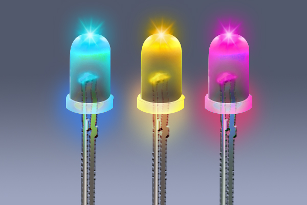
Electroluminescence (LEDs): Under forward bias of a p–n junction, minority carriers are injected and undergo radiative recombination in the junction region, emitting light (spontaneous emission).
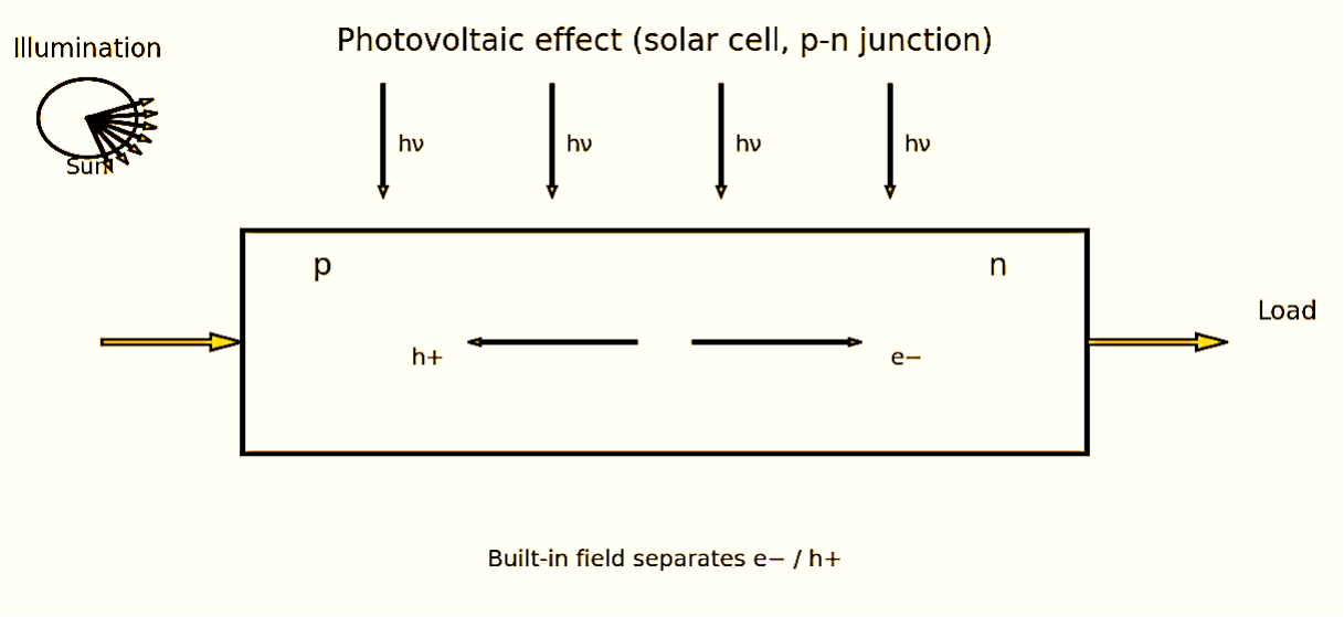
Photovoltaic effect (solar cells): Photons incident on a p–n or p–i–n structure generate electron–hole pairs in the active layer; the junction’s built-in electric field drives electrons toward the n-side and holes toward the p-side, producing a photocurrent. With an external load connected, the device delivers current and voltage, thus converting light energy directly into electrical energy.
States of Matter and Plasma
Common States of Matter
· Solid: Fixed shape and volume; can be crystalline (ordered) or amorphous/glassy (no long-range order). Particles primarily undergo thermal vibrations about equilibrium positions.
· Liquid: Fixed volume but no fixed shape; flows readily. Density is close to that of solids and far higher than that of gases; nearly incompressible.
· Gas: No fixed shape or volume; easily compressed and highly diffusive.
Other Important Phases
· Plasma: A quasi-neutral ionized gas composed of electrons, ions, excited species, and neutral particles, exhibiting high electrical conductivity and collective behavior. It can be produced at high temperatures or by applying RF/microwave/DC electric fields to a low-pressure gas to induce breakdown.
· Superconducting state / Superfluid: Characterized by zero electrical resistance / flow without viscosity, respectively.
· Liquid crystals, supercritical fluids, Bose–Einstein condensates, supersolids, and others are additional special phases.
Applications of Plasma in Semiconductors and Beyond
· Semiconductor manufacturing: RIE (reactive ion etching) / ICP (inductively coupled plasma) etching; PECVD (plasma-enhanced chemical vapor deposition) / PEALD (plasma-enhanced atomic layer deposition) thin-film growth; surface cleaning and activation. Plasma supplies reactive species/free radicals and ion bombardment to accelerate reactions and enable anisotropic processing.
· Lighting & displays: Fluorescent lamps, neon signs (historically, plasma displays).
· Aerospace: Hall thrusters and ion propulsion.
· Research & energy: Controlled nuclear fusion and plasma physics.
· Environmental: Low-temperature plasma treatment of exhaust gases/VOCs (volatile organic compounds).
Aladdin Semiconductor Raw Materials List
Category | Name | Use | Catalog No. | Specification |
Wet Electronic Chemicals | Hydrogen peroxide | Cleaning and etching of silicon materials | H433855 | ≥99.999% metals basis; contains potassium stannate inhibitor; semiconductor grade; 30–32 wt.% in water |
Wet Electronic Chemicals | Hydrofluoric acid (HF) | Etching SiO₂ and cleaning quartzware | H116237 | Semiconductor grade, PrimorTrace™ Ultra; ≥99.99998% metals basis; 49 wt.% in H₂O |
Wet Electronic Chemicals | Sulfuric acid (H₂SO₄) | “Piranha” solution (7 parts H₂SO₄ : 3 parts 30% H₂O₂) for wafer cleaning | S399876 | PrimorTrace™; ≥99.999% metals basis |
Wet Electronic Chemicals | Phosphoric acid (H₃PO₄) | Etching silicon nitride (Si₃N₄) | P123765 | Semiconductor grade |
Wet Electronic Chemicals | Hydrochloric acid (HCl) | Wet clean chemistry; part of SC-2 for removing heavy metals from silicon | H466585 | PrimorTrace™; ≥99.999% metals basis; 37 wt.% in H₂O |
Wet Electronic Chemicals | Nitric acid (HNO₃) | Mixed with HF (HNA) for silicon chemical etch/polish; PSG removal typically uses HF/BOE | N116245 | PrimorTrace™; ≥99.999% metals basis; 70% |
Wet Electronic Chemicals | Acetic acid (glacial) | Wafer cleaning, photoresist removal, and etch processes | A116171 | Semiconductor grade; ≥99.7% |
Wet Electronic Chemicals | Ammonium hydroxide (NH₄OH) | Cleaning agent | A431915 | ≥99.99% metals basis; 28–30% NH₃ in H₂O |
Wet Electronic Chemicals | Sodium hydroxide (NaOH) | Wet etching | S163080 | Semiconductor grade; ≥99.9% metals basis |
Wet Electronic Chemicals | Tetramethylammonium hydroxide (TMAH) | Positive photoresist developer | Ultra-pure (trace analysis); 25% aqueous stock (commonly diluted to 2.38 wt.% for development) | |
Wet Electronic Chemicals | Potassium hydroxide (KOH) | Anisotropic wet etching of silicon (common in MEMS) | Semiconductor grade; ≥99.999% metals basis; sodium-free | |
Wet Electronic Chemicals | Deionized water (DI) | Widely used for wafer rinsing and diluting cleaners | W119424 | Deionized |
Wet Electronic Chemicals | Isopropanol (IPA) | General-purpose cleaner | I419710 | PrimorTrace™; semiconductor grade; ≥99.999% metals basis |
Wet Electronic Chemicals | Acetone | General-purpose cleaner (stronger than IPA) | A399711 | UltraPureChrom™; HPLC grade for liquid chromatography; ≥99.9% |
Wet Electronic Chemicals | Trichloroethylene (TCE) | Solvent for wafer/general cleaning | ACS; ≥99.5% | |
Wet Electronic Chemicals | Xylene | Removal of surface contaminants and photoresist | ACS; ≥98.5% (isomers plus ethylbenzene) | |
Substrate Materials | Ferrocene | Fe dopant precursor (to form semi-insulating compound semiconductors) | ≥99% | |
Substrate Materials | Bis-cyclopentadienyl magnesium (Cp₂Mg) | GaN p-type dopant precursor (MOCVD) | ≥99.9998% metals basis | |
Substrate Materials | Titanium (Ti) | Fabrication of transistors, resistors, capacitors, etc. | T109127 | PrimorTrace™; ≥99.99% metals basis; powder, ≥300 mesh |
Substrate Materials | Hafnium (Hf) | Fabrication of transistors, resistors, capacitors, etc. | H106102 | ≥99.9% metals basis; 1–10 mm |
Substrate Materials | Aluminum (Al) | Fabrication of transistors, resistors, capacitors, etc. | PrimorTrace™; ≥99.999% metals basis; pellets, 3–8 mesh | |
Substrate Materials | Phosphorus (P) | Fabrication of transistors, resistors, capacitors, etc. | P104469 | PrimorTrace™; ≥99.999% metals basis; lumps, 1–5 mm |
Substrate Materials | Boron (B) | Fabrication of transistors, resistors, capacitors, etc. | PrimorTrace™; ≥99.99% metals basis; powder, ≥300 mesh | |
Substrate Materials | Selenium (Se) | Fabrication of transistors, resistors, capacitors, etc. | PrimorTrace™; ≥99.999% metals basis; D50 ≥80 mesh | |
Substrate Materials | Tellurium (Te) | Fabrication of transistors, resistors, capacitors, etc. | T130110 | PrimorTrace™; ≥99.999% metals basis; ≥100 mesh |
Substrate Materials | Diamond | Fabrication of transistors, resistors, capacitors, etc. | N140012 | ≥99%; 30–50 nm |
Substrate Materials | Germanium (Ge) | Fabrication of transistors, resistors, capacitors, etc. | C105151 | PrimorTrace™; ≥99.999% metals basis; 1–3 mm |
Substrate Materials | Gallium (Ga) | Fabrication of transistors, resistors, capacitors, etc. | G105132 | PrimorTrace™ Ultra; ≥99.99999% metals basis |
Substrate Materials | Tin (Sn) | Fabrication of transistors, resistors, capacitors, etc. | PrimorTrace™; ≥99.999% metals basis; granular, 1–6 mm | |
Substrate Materials | Silicon (Si) | Mainstream CMOS | PrimorTrace™; ≥99.99% metals basis; 1–3 mm | |
Substrate Materials | Silicon carbide (SiC) | Wide bandgap; suitable for harsh environments | ≥99.9% metals basis | |
Substrate Materials | Gallium nitride (GaN) | Commonly grown epitaxially on Si or sapphire | G119228 | PrimorTrace™; ≥99.99% metals basis |
Substrate Materials | Gallium arsenide (GaAs) | High electron mobility | G119227 | PrimorTrace™; ≥99.999% metals basis; pieces |
Substrate Materials | Indium phosphide (InP) | Lasers, modulators, high-frequency devices | ≥99.998% metals basis; 3–20 mesh | |
Dielectric Materials | Silicon dioxide (SiO₂) | Gate oxide, interlayer dielectric, isolation | ≥99.9% metals basis; spheres, 35 μm | |
Dielectric Materials | Silicon nitride (Si₃N₄) | Passivation, spacers | ≥99.9% metals basis; α-phase |
Aladdin: https://www.aladdinsci.com/